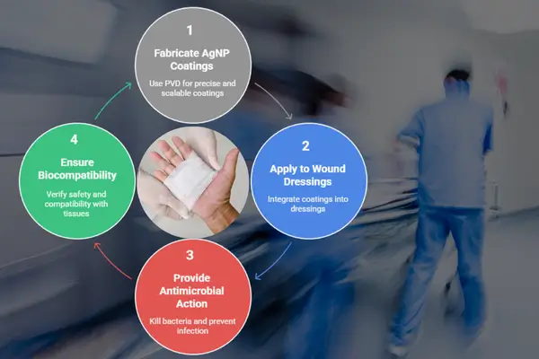
Blog

High-Temperature Superconductors Shaping the Future of Quantum Materials

High-Temperature Superconductors Shaping the Future of Quantum Materials

Plasmonics, the study of light interacting with free electrons on metal surfaces, has become an essential tool for advancing quantum technologies. By exploiting the unique properties of plasmonic materials, typically metals such as gold, silver, and copper, researchers have opened new avenues for improving the sensitivity, precision, and capabilities of quantum systems. In particular, the […]

High-Temperature Superconductors Shaping the Future of Quantum Materials Read More »

Plasmonic Interactions in Quantum Sensing _nikalyte

Plasmonic Interactions in Quantum Sensing Materials

Plasmonics, the study of light interacting with free electrons on metal surfaces, has become an essential tool for advancing quantum technologies. By exploiting the unique properties of plasmonic materials, typically metals such as gold, silver, and copper, researchers have opened new avenues for improving the sensitivity, precision, and capabilities of quantum systems. In particular, the

Plasmonic Interactions in Quantum Sensing Materials Read More »

Surface-Enhanced Raman Scattering (SERS) for Biosensing Applications

SERS for Biosensing Applications

Surface-Enhanced Raman Scattering (SERS) has rapidly gained recognition as a groundbreaking biosensing technique, enabling the accurate, rapid, and non-invasive detection of diseases, pathogens, and environmental toxins. By significantly amplifying Raman signals through nanomaterials, SERS makes it possible to detect trace amounts of biological analytes, positioning it as a leading method for medical diagnostics, food safety,

SERS for Biosensing Applications Read More »

What is Electron Beam Evaporation?

Electron Beam Evaporation (E-Beam Evaporation) is a precise Physical Vapor Deposition (PVD) process used for applying high-density, thin coatings to substrates. E-Beam Evaporation operates under high vacuum conditions and employs a focused electron beam to evaporate the coating material (source material), which is then deposited onto a substrate.[1] This deposition method is essential for industries

What is Electron Beam Evaporation? Read More »

Fuel Cell_Nikalyte_PCS

The Benefits of PVD for Chemical-Free Powder Coatings

Powder coating has become a preferred method for enhancing functionality and applying durable finishes to a variety of substrates, from automotive components to industrial machinery.  However, the latest advancements in PVD (Physical Vapor Deposition) technology are transforming the way we think about coating processes. This innovative approach not only improves the quality and precision of

The Benefits of PVD for Chemical-Free Powder Coatings Read More »

UHV Epitaxy of Oxides and III-V Nitrides

RF Atom Sources for UHV Epitaxy of Oxides & III-V Nitrides

In today’s race for faster, more efficient semiconductors and advanced electronic materials, true innovation begins at the atomic scale. Whether it’s next-generation optoelectronics, wide-bandgap power devices, or quantum materials, the performance of these technologies depends on the precision and purity of their thin-film layers. The RF (Radio Frequency) Atom Source has become a pivotal component

RF Atom Sources for UHV Epitaxy of Oxides & III-V Nitrides Read More »

Graph illustrating Lift off process using E-beam deposition(adapted from Eschimese, D., Vaurette, F., Troadec, D., Leveque, G., Melin, T., and Arscott, S., "Size and shape control of a variety of metallic nanostructures using tilted, rotating evaporation and lithographic lift-off techniques," Scientific Reports, 9, 14058, 2019, DOI: https://www.nature.com/articles/s41598-019-44074-w

Lift-Off Process for Nanoscale Devices Using E-Beam Deposition

Image courtesy: Lift off process using E-beam deposition (adapted from Eschimese, D., Vaurette, F., Troadec, D., Leveque, G., Melin, T., and Arscott, S., “Size and shape control of a variety of metallic nanostructures using tilted, rotating evaporation and lithographic lift-off techniques,” Scientific Reports, 9, 14058, 2019, DOI: https://www.nature.com/articles/s41598-019-44074-w The lift-off process is one of the

Lift-Off Process for Nanoscale Devices Using E-Beam Deposition Read More »

A practical guide to magnetron-based thin film deposition

Thin films are at the heart of modern technology, used in everything from semiconductor devices to optical coatings and protective layers. Magnetron-based thin film deposition is one of the most effective methods for producing high-quality coatings with exceptional uniformity, adhesion, and material control. By utilizing plasma to transfer material from a target onto a substrate,

A practical guide to magnetron-based thin film deposition Read More »

Superior thin film Coatings with Multi-Target Sputtering

In thin film deposition, precision and control are critical for producing high-performance coatings that meet the rigorous demands of industries such as semiconductors, optics, and materials science. Multi-target sputtering, particularly systems with three target configurations, has emerged as a transformative solution to enhance deposition versatility, material composition, and process control. The Need for Multi-Target Sputtering

Superior thin film Coatings with Multi-Target Sputtering Read More »

Why RF sputter deposition is used for dielectrics

Dielectric materials are the foundation of modern electronics, acting as insulators in circuits, capacitors, and semiconductor devices. Their ability to store and manage electric fields makes them indispensable in everything from microchips to high-frequency communication systems. However, producing high-quality dielectric films with the required precision and uniformity is a challenge. Among the thin-film deposition techniques,

Why RF sputter deposition is used for dielectrics Read More »

Scroll to Top