Want to read offline? [Download PDF]
Electron Beam Evaporation (E-Beam Evaporation) is a precise Physical Vapor Deposition (PVD) process used for applying high-density, thin coatings to substrates. E-Beam Evaporation operates under high vacuum conditions and employs a focused electron beam to evaporate the coating material (source material), which is then deposited onto a substrate.[1] This deposition method is essential for industries where material properties like conductivity, optical characteristics, and mechanical durability are critical.
In this blog, we’ll explore the E-Beam Evaporation process, its key components, advantages, disadvantages, and how it compares to other thin-film deposition techniques.
How Does E-Beam Evaporation Work?
E-Beam Evaporation is a high-precision thin-film deposition technique where the source material is subjected to a high-power electron beam. The process works as follows:
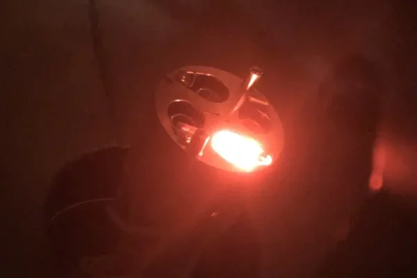
- Electron Beam Generation: A tungsten filament is heated to over 2,000°C, generating a stream of high-energy electrons.
- Target Material Heating: The electron beam is focused on the source material (held in a crucible), causing it to evaporate.
- Deposition on Substrate: The evaporated atoms travel through the vacuum chamber and condense onto a substrate, forming a thin film, typically in the nanometre range (5 to 250 nm).
- Real-Time Monitoring: Quartz crystal microbalances (QCM) or optical sensors track the thickness of the deposited film in real-time, ensuring precise control over the layer’s uniformity and thickness.
This direct transfer of energy to the source material makes E-Beam Evaporation especially suitable for high-melting-point materials that would be difficult to vaporize using conventional heating methods like thermal evaporation.[2]
Materials for E-Beam Evaporation
E-Beam Evaporation can be used with a wide range of source materials and substrates:
Source Materials | Substrates |
Metals: Gold (Au), Silver (Ag), Copper (Cu), Nickel (Ni), Titanium (Ti), Chromium (Cr) | Silicon Wafers: Common in semiconductor and microelectronics applications. |
Refractory Metals: Tungsten (W), Tantalum (Ta) | Glass, Ceramics, and Quartz: Used for optical coatings and decorative films. |
Dielectrics: Indium Tin Oxide (ITO), Silicon Dioxide (SiO2), Magnesium Fluoride (MgF2) | Sapphire: Ideal for high-performance optical components and LEDs |
Advantages of E-Beam Evaporation
E-Beam Evaporation offers several key benefits in thin-film deposition:
- High Deposition Rates: E-Beam Evaporation allows rapid vapor deposition rates from 0.1 μm/min to 100 μm/min, resulting in fast and efficient production of thin films.
- High Purity Coatings: Due to the direct heating of the source material, contamination from the crucible is minimized, leading to high-purity films.
- Material Flexibility: E-Beam Evaporation is compatible with a wide range of materials, including high-temperature metals, refractory metals, dielectrics, and precious metals. Materials like gold, silver, tungsten, indium tin oxide (ITO), and silicon dioxide can be deposited with precision.
- Multi-Layer Deposition: E-Beam systems with multiple crucibles allow for multi-layer deposition without the need to vent the system, making it ideal for complex coatings.
- High Material Utilization: The process achieves high material utilization efficiency, minimizing waste and reducing operational costs.
Disadvantages of E-Beam Evaporation
Despite its numerous advantages, there are some limitations to the E-Beam Evaporation process:
- Cost and Complexity: The E-Beam Evaporation system is complex and expensive, requiring specialized equipment and significant energy input.
- Substrate Geometry Limitations: The process is best suited for line-of-sight substrates, making it less effective for coating substrates with complex geometries.
- Filament Degradation: The electron filament can degrade over time, leading to non-uniform evaporation rates and potential inconsistencies in film deposition.
- Heat load on substrate: E-beam evaporation can introduce localized heating on the substrate, which may lead to thermal stresses or damage, especially for temperature-sensitive materials. This can affect the quality and uniformity of the deposited thin films, requiring careful temperature control and substrate management.
E-Beam Evaporation Applications
E-Beam Evaporation is employed in a wide range of industries, including:
- Aerospace: To apply temperature-resistant coatings on components, enhancing their durability in extreme conditions. [3]
- Semiconductors and Electronics: For thin-film deposition on semiconductor wafers, integrated circuits, and solar cells.[4]
- Optical Coatings: Applied for optical filters, anti-reflective coatings, and mirrors.[5]
- Tool Coatings: Hard, wear-resistant coatings for tools in industries requiring durability.[6]
E-Beam Evaporation vs. Other PVD Techniques
E-Beam Evaporation competes with other Physical Vapor Deposition (PVD) techniques, such as thermal evaporation, and sputtering. Let’s compare E-Beam Evaporation with these processes
Criteria | E-Beam Evaporation vs. Thermal Evaporation | E-Beam Evaporation vs. Sputtering |
Deposition Rate | Higher in E-Beam Evaporation compared to Thermal Evaporation. | Higher in E-Beam Evaporation compared to Sputtering. |
Material Compatibility | E-Beam Evaporation can handle high-melting-point materials like metal oxides. | Sputtering is more effective for coating complex geometries and large-area substrates, while E-Beam Evaporation is optimized for line-of-sight deposition. |
Film Density | E-Beam Evaporation produces denser thin films with fewer impurities. | E-Beam Evaporation results in in films with higher density compared to sputtering, especially when the material has a high melting point. This is because the vaporized material is generally in a neutral atomic or molecular state, leading to a more compact and dense film structure as the particles condense directly onto the substrate. |
Heating Method | E-beam uses a high-power electron beam to directly heat the material. Thermal evaporation uses an electric current to heat the crucible. | Unlike E-Beam Evaporation, sputtering uses plasma atoms (typically argon) to dislodge material from a negatively charged target. |
Purity | E-beam has higher purity due to minimized contamination from the crucible. | E-Beam Evaporation typically provides higher purity than Sputtering. |
E-Beam Hearth vs. Mini E-Beam Evaporators
E-beam hearth evaporators use focused electron beams to heat and vaporize materials, enabling precise thin-film deposition at high rates. These systems are ideal for large-scale industrial applications, such as semiconductor fabrication, optical coatings, and photovoltaic manufacturing, offering high material versatility and excellent control over deposition rates and film quality.
In contrast, mini e-beam evaporators heat and vaporize materials by focusing a high-energy electron beam onto a target, rapidly heating the material to its evaporation point, and allowing precise thin-film deposition on substrates. Unlike traditional thermal evaporation systems, mini e-beam evaporators do not require a boat to hold the material. Instead, the material is directly heated by the electron beam. They are compact, cost-effective solutions designed for small-scale production, R&D, and prototyping. They provide precise thin-film deposition with reduced energy consumption, making them perfect for laboratory settings or low-volume manufacturing. While they offer slower deposition rates compared to full-sized systems, their efficiency, precision, and ease of use make them an attractive choice for niche applications and smaller projects. We offer the Evap-4 Mini e-beam evaporator, designed for high precision and cost-effective thin-film deposition in research and small-scale production environments.
Conclusion
Electron Beam Evaporation is an indispensable PVD technique for producing high-quality thin films with precise control over material properties. Its ability to handle high-melting-point materials and deliver dense, high-purity films makes it ideal for industries such as aerospace, semiconductor manufacturing, and optics. By understanding the benefits, limitations, and comparison with other deposition techniques, engineers can make informed decisions to meet the demanding requirements of advanced manufacturing and research applications.
Contact us to speak to one of our technical experts about the Evap-4 Mini e-beam evaporator.
References:
- Van Dorp, W. F., & Hagen, C. W. (2008). A critical literature review of focused electron beam induced deposition. Journal of Applied Physics, 104(8), 081301. https://doi.org/10.1063/1.2977587
- Maiti, N., Karmakar, P., Barve, U. D., & Bapat, A. V. (2008). An evaporation system for film deposition using electron beam sources. Journal of Physics: Conference Series, 114, 012049. https://doi.org/10.1088/1742-6596/114/1/012049
- Vasile, B. S., Birca, A. C., Surdu, V. A., Neacsu, I. A., & Nicoară, A. I. (2020). Ceramic composite materials obtained by electron-beam physical vapor deposition used as thermal barriers in the aerospace industry. Nanomaterials, 10(2), 370. https://doi.org/10.3390/nano10020370
- Matkivskyi, V., Lee, Y., Seo, H. S., Lee, D.-K., Park, J.-K., & Kim, I. (2021). Electronic-beam evaporation processed titanium oxide as an electron selective contact for silicon solar cells. Current Applied Physics, 29, 202-206. https://doi.org/10.1016/j.cap.2021.10.005
- Chen, Y.-L., & Wang, P.-J. (2023). Study of ion-assisted E-beam evaporation coating process on chirped mirrors. Coatings, 13(2), 356. https://doi.org/10.3390/coatings13020356
- Caliskan, H., Panjan, P., & Kurbanoglu, C. (2020). Hard coatings on cutting tools and surface finish. In Handbook of Surface Treatment and Finishing (pp. 439-457). Elsevier. https://doi.org/10.1016/B978-0-12-803581-8.09178-5