Image courtesy: Lift off process using E-beam deposition (adapted from Eschimese, D., Vaurette, F., Troadec, D., Leveque, G., Melin, T., and Arscott, S., “Size and shape control of a variety of metallic nanostructures using tilted, rotating evaporation and lithographic lift-off techniques,” Scientific Reports, 9, 14058, 2019, DOI: https://www.nature.com/articles/s41598-019-44074-w
Want to read offline? [Download PDF]
The lift-off process is one of the most crucial techniques in the fabrication of nanoelectronics and quantum devices. With the increasing demand for precise, high-performance devices in semiconductor manufacturing, MEMS, and quantum computing, achieving the highest level of accuracy is non-negotiable. The Nikalyte Mini E-Beam Evaporator EVAP-4 is an industry-leading e-beam deposition tool that excels at delivering high-precision thin film deposition and the superior material quality required for advanced nanoelectronics and quantum device applications.
What is the Lift-Off Process in Nanoelectronics and Quantum Devices?
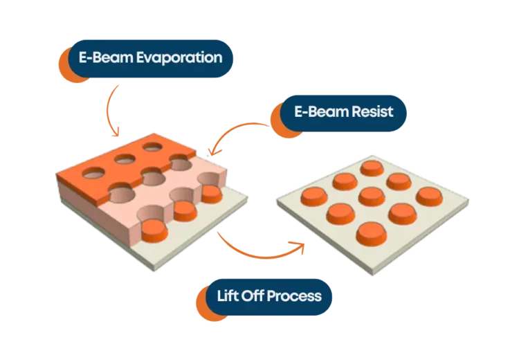
The lift-off process is a widely used technique in nanoelectronics fabrication and quantum device manufacturing. It involves patterning thin films on substrates to create precise, fine patterns for interconnects, contacts, and other critical components. The key steps in the lift-off process are:
- Photoresist Coating: A photoresist material is applied to the substrate. This material is sensitive to light or electron beams and can be patterned to define areas for material deposition. [1]
- Pattern Development: After exposing the photoresist to light or an electron beam, the exposed areas are developed, leaving a mask that will protect parts of the substrate from material deposition. [2]
- Material Deposition: E-beam evaporation is commonly used to deposit thin layers of material, including metals, dielectrics, and semiconductors, onto the substrate.[3]
- Lift-Off: The photoresist is dissolved, “lifting off” the unwanted material and leaving behind only the desired pattern.[4]
This lift-off technique is vital for achieving the precision required for nanoelectronics and quantum devices, where extremely fine features are needed to ensure device functionality and performance.
Why choose Nikalyte Mini E-Beam Evaporator EVAP-4?
The Nikalyte Mini E-Beam Evaporator EVAP-4 is a state-of-the-art tool designed to offer high-precision material deposition during the lift-off process. As a compact yet highly efficient e-beam evaporator, the EVAP-4 provides superior performance in both nanoelectronics manufacturing and quantum device fabrication. Here’s how it enhances the lift-off process:
High-Precision Material Deposition:
The EVAP-4 delivers high-precision material deposition for creating well-defined patterns on the substrate, which is essential for nanoelectronics and quantum devices. Whether you’re working with metals like gold, aluminium, titanium, or semiconductors and dielectrics, the e-beam evaporator ensures precise control over material thickness, leading to consistent and reliable patterns.[5]This level of precision is vital for quantum computing devices like superconducting qubits or quantum dots, where even the smallest variation can affect device performance.[6]
Superior Thin Film Quality :
The EVAP-4 ensures the creation of high-quality thin films that are smooth, uniform, and free from contamination. The high-vacuum environment of the e-beam evaporator minimizes impurities during deposition, allowing for better material adhesion and improved electrical properties. This is especially important for quantum devices, where maintaining the coherence of quantum states is critical for device functionality.
Flexibility for Multi-Material Deposition:
Nanoelectronics and quantum devices often require the deposition of multiple materials, such as metals for interconnects, dielectrics for insulation, and semiconductors for active layers. The EVAP-4 can handle all of these materials with ease, allowing for the creation of multi-layered devices.[7]For example, in a superconducting qubit fabrication process, layers of superconducting metals like niobium or aluminium are deposited using e-beam evaporation, followed by dielectric layers for isolation and control. The EVAP-4 ensures that each layer is deposited with the required uniformity and precision, facilitating the lift-off process to achieve the desired patterning and device structure.[8]
Repeatability for precise Fabrication:
The system’s automated control over deposition parameters like material flux, current, and time ensures that each deposition process is repeatable and consistent.[5] For nanoelectronics, repeatability is important for ensuring that every chip or wafer has the same precise features. In quantum device fabrication, repeatability ensures that quantum devices are manufactured to consistent standards, reducing variability and increasing reliability.[9]
Compact and Cleanroom-Compatible Design:
The EVAP-4 is designed with a compact footprint, making it an excellent choice for cleanroom environments where space is often at a premium. Its cleanroom compatibility ensures that there is minimal contamination during the e-beam evaporation process, which is crucial when working at the nanoscale. This feature is especially important in the development of high-performance quantum devices and nanoelectronics.
Applications of the Lift-Off Process in Nanoelectronics and Quantum Devices
The lift-off process plays a critical role in fabricating nanoelectronics such as field-effect transistors (FETs), capacitors, resistors, and integrated circuit interconnects. The lift-off process, combined with the capabilities of the EVAP-4, ensures that nanoelectronic devices can be produced at a scale suitable for mass production, with the accuracy required for high-performance applications in consumer electronics, telecommunications, and computing.[10] The lift-off process is also fundamental for creating quantum devices like superconducting qubits and quantum dots. The ability to deposit superconducting metals and dielectric layers with extreme precision is essential for creating quantum circuits that can operate at the low temperatures and high coherence required for quantum computing applications. The EVAP-4 enables the reliable deposition of multiple materials required for quantum device fabrication, facilitating the development of advanced quantum computing technology.
Conclusion
The Nikalyte Mini E-Beam Evaporator EVAP-4 is a state-of-the-art tool that elevates the lift-off process, enabling high-precision deposition for the most advanced nanoelectronics and quantum devices. With its ability to handle multiple materials, ensure superior thin film quality, and offer repeatability for scalable production, the EVAP-4 is the go-to solution for researchers and manufacturers in these fields. From fabricating nanoelectronic components to advancing quantum device development, the EVAP-4 is instrumental in shaping the future of next-generation technology.
References:
- Chen, Y., “Nanofabrication by electron beam lithography and its applications: A review,” Vac. Sci. Technol. B, 34, 020801 (2016). https://www.sciencedirect.com/science/article/abs/pii/S016793171500101X?via%3Dihub
- Franssila, S., Introduction to Microfabrication, 2nd ed., Wiley, 2010. https://doi.org/10.1002/9781119990413
- Mühlberger, M., ed., Nanoimprint Lithography: Technology and Applications, MDPI, 2022. https://doi.org/10.3390/books978-3-0365-4481-6
- Wang, Z., and Zhang, Z., “Electron Beam Evaporation Deposition,” in Title of the Book, edited by Y. Lin and X. Chen, Wiley-VCH, 2016, https://doi.org/10.1002/9783527696406.ch2
- Nikalyte Ltd. (2021). Mini E-Beam Evaporator EVAP-4 Technical Specifications. Retrieved from Nikalyte Website
- Balamurugan, S., Sivakami, A., Mathankumar, M., Prasad, Y., and Ahmad, I., “Quantum computing basics, applications and future perspectives,” Journal of Molecular Structure, 1308, 137917 (2024).https://doi.org/10.1016/j.molstruc.2024.137917
- Sarkar, A., Sarkar, C. K., and Benfdila, A., eds., Nanoelectronics: Physics, Materials, and Devices, Elsevier, 2023. https://shop.elsevier.com/books/nanoelectronics-physics-materials-and-devices/sarkar/978-0-323-91832-9
- Barcelo, S., and Li, Z., “Nanoimprint lithography for nanodevice fabrication,” Nano Convergence, 3, 21 (2016). https://link.springer.com/article/10.1186/s40580-016-0081-y
- Gao, Y. Y., Rol, M. A., Touzard, S., and Wang, C., “Practical guide for building superconducting quantum devices,” PRX Quantum, 2, 040202 (2021). https://doi.org/10.1103/PRXQuantum.2.040202
- Tseng, A., Chen, K., Chen, C., and Ma, K. J., “Electron beam lithography in nanoscale fabrication: recent development,” IEEE Transactions on Electronics Packaging Manufacturing, 26(2), 141-149 (2003). https://doi.org/10.1109/TEPM.2003.817714