Want to read offline? [Download PDF]
Thin Film Lithium Niobate (TFLN) has become one of the most sought-after materials in modern photonics and integrated optoelectronics. With applications in telecommunications, quantum computing, photonic integrated circuits (PICs), and high-frequency electro‑optic modulators, TFLN is increasingly recognised as a cornerstone material for next‑generation optical technologies. [1],[2] Among available physical vapour deposition (PVD) techniques, magnetron sputtering stands out as a particularly effective approach, offering precise control over film composition, excellent thickness uniformity, scalability, and compatibility with industrial manufacturing processes. [3], [4]
Why TFLN Matters
Lithium niobate (LiNbO₃) exhibits outstanding electro‑optic, acousto‑optic, and nonlinear optical properties, including a high Pockels coefficient and wide optical transparency window.[1] When implemented in thin‑film form, these properties are significantly enhanced by strong optical confinement, enabling compact, low‑loss, and high‑speed integrated photonic devices.[2]
Recent experimental demonstrations show that TFLN‑based photonic computing circuits can achieve processing speeds of 43.8 GOPS per channel with an energy consumption as low as 0.0576 pJ per operation, highlighting the suitability of TFLN for energy‑efficient optical computing and signal processing.[5] These characteristics are particularly attractive for telecommunications networks, hyperscale data centres, and emerging AI hardware accelerators.
State‑of‑the‑art TFLN modulators have demonstrated data transmission rates exceeding 400 Gbit/s and are regarded as enabling components for future 1.6 Tbps and 3.2 Tbps optical switching architectures.[2],[6] Furthermore, energy efficiency is a critical driver: large‑scale computing facilities allocate approximately 40–45% of their total energy consumption to cooling, whereas photonic systems based on electro‑optic materials such as TFLN dissipate negligible heat during operation.[5]
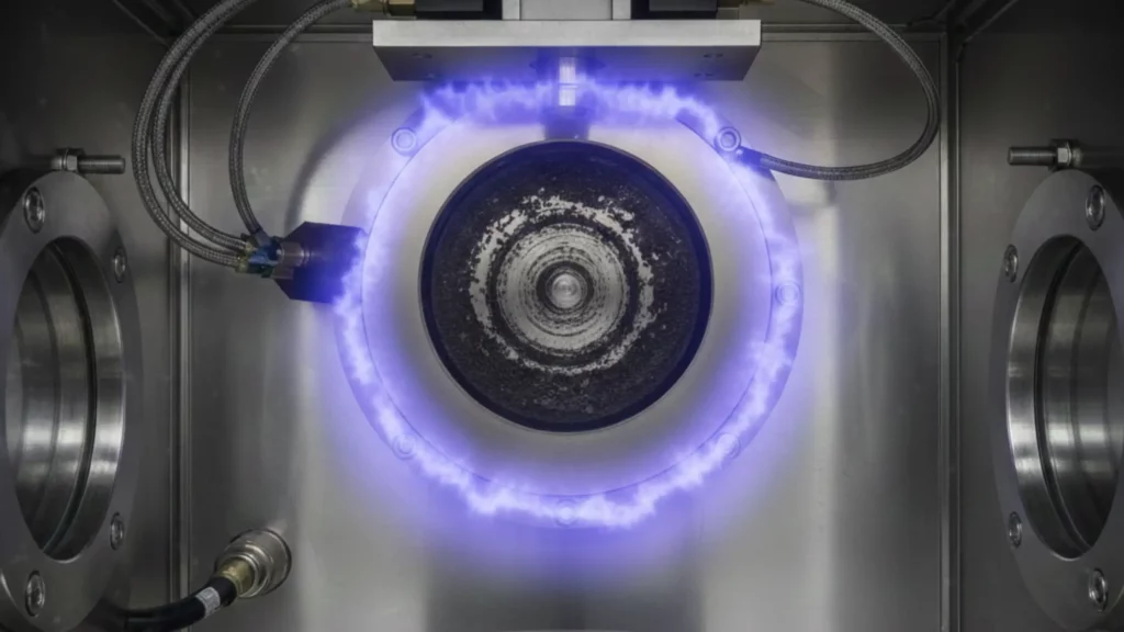
Why Magnetron Sputtering Is a Preferred Method for TFLN
Magnetron sputtering offers several advantages for TFLN deposition, including room‑temperature deposition capability, high film density, uniform thickness control over large areas, and strong adhesion to a wide range of substrates. [3], [4] In this process, energetic ions generated in a plasma bombard a lithium niobate target, ejecting atoms that subsequently condense onto the substrate surface. The application of a magnetic field confines electrons near the target, enhancing ionisation efficiency and enabling stable, high‑rate deposition.
Radio‑frequency (RF) magnetron sputtering operating at 13.56 MHz is the dominant technique for depositing lithium niobate thin films, as it mitigates charge accumulation on insulating ceramic targets by periodically reversing the electric field. [3],[7] Reported deposition parameters typically include RF powers between 40 and 100 W, working pressures of 10–20 mTorr, substrate temperatures ranging from room temperature up to 800 °C, and argon‑to‑oxygen gas ratios close to 1:1 to promote stoichiometric oxide formation.[8]
Critical Deposition Challenges
- Stoichiometry Control: Maintaining correct stoichiometry remains the primary challenge in TFLN deposition. Lithium niobate is a non‑line compound, and small deviations in the Li/Nb ratio can result in secondary phases such as LiNb₃O₈ (Nb‑rich) or Li₃NbO₄ (Li‑rich), which degrade optical performance.[1] Lithium’s high vapour pressure leads to preferential loss during deposition, often producing lithium‑deficient films. Experimental studies demonstrate that reactive co‑sputtering using separate lithium‑ and niobium‑containing targets offers superior stoichiometric control compared with single‑target sputtering. [9]
- Phase Formation and Crystallinity: Achieving single‑phase, highly crystalline LiNbO₃ thin films requires careful optimisation of deposition and post‑treatment conditions. Multiple Li–Nb–O phases have been reported as a function of oxygen partial pressure, substrate temperature, and plasma energy. [1],[3] Post‑deposition annealing at temperatures between 700 °C and 950 °C is widely reported to enhance crystallinity, reduce defect density, and improve electro‑optic performance, although optimal conditions depend strongly on substrate choice and film thickness. [10]
- Target Cooling and Uniformity: Thermal management of the LiNbO₃ target is essential for stable deposition. Insufficient cooling can lead to target cracking, non‑uniform sputtering, and unintended phase formation. Advanced magnetron sputtering systems incorporate efficient water‑cooled backing plates and real‑time thermal monitoring to maintain consistent target temperatures throughout long deposition runs. [11]
Recent Progress in RF magnetron sputtering for TFLN films
Recent advances in RF magnetron sputtering have enabled the deposition of high‑quality TFLN films with thicknesses in the range of 300–350 nm on sapphire and x‑cut lithium niobate substrates at substrate temperatures as low as 280 °C.[8] For photonic integrated circuit applications, X‑ray diffraction full‑width at half‑maximum (FWHM) values as low as 0.35° for (006)‑oriented LiNbO₃ films have been reported, indicating crystalline quality suitable for low‑loss optical waveguides. [10] Surface roughness values below 6 nm are commonly targeted to minimise scattering losses in guided‑wave devices. [7]
Process Optimisation Essentials
- Substrate Selection: Common substrates include silicon (111) and (100), c‑plane and r‑plane sapphire, x‑, y‑, and z‑cut lithium niobate crystals, and platinised silicon. Surface cleaning and pre‑treatment are essential for achieving strong adhesion and uniform nucleation.[1]
- Gas Composition: Argon‑to‑oxygen ratios close to 1:1 at working pressures of 10–20 mTorr are widely reported to yield near‑stoichiometric films.[8]
- Power Management: Power densities of approximately 20 W/in² or lower are recommended for bonded ceramic targets to prevent debonding, while unbonded targets can tolerate higher power densities with target utilisation of up to 40%. [11]
- In‑situ Monitoring: Optical emission spectroscopy, quartz crystal microbalance sensors, substrate temperature probes, and residual gas analysis are routinely employed for real‑time plasma and process control in advanced sputtering systems. [3]
Challenges in Thin Film Lithium Niobate Deposition via Magnetron Sputtering
Depositing high-quality thin film lithium niobate (TFLN) via magnetron sputtering presents several critical challenges that directly impact the performance of photonic devices. The most significant hurdle is stoichiometry control, maintaining the precise Li/Nb ratio is notoriously difficult because lithium’s high vapor pressure leads to preferential loss during deposition, often producing lithium-deficient films. Even minor deviations in stoichiometry can generate unwanted secondary phases such as LiNb₃O₈ (niobium-rich) or Li₃NbO₄ (lithium-rich), which degrade optical performance. To address this challenge, reactive co-sputtering using separate lithium and niobium-containing targets offers superior stoichiometric control compared with single target sputtering.[9] Beyond stoichiometry, thermal management of the LiNbO₃ target is essential for stable deposition, as insufficient cooling can lead to target cracking, non-uniform sputtering, and unintended phase formation.[11] Post-deposition annealing at temperatures between 700°C and 950°C is widely reported to enhance crystallinity, reduce defect density, and improve electro-optic performance. [10] These interconnected challenges underscore why TFLN deposition demands precise parameter optimization and advanced equipment capable of real-time plasma monitoring.
Why Choose Nikalyte for Thin Film Lithium Niobate Deposition
Nikalyte’s advanced PVD systems are engineered to address the stringent requirements of TFLN deposition. The NEXUS ultra‑high vacuum system operates at base pressures down to 5 × 10⁻⁷ Torr, minimising contamination and enabling high‑purity film growth, while supporting substrate heating up to 800 °C for crystallinity optimisation. [12] Multi‑target configurations enable precise stoichiometry control through reactive co‑sputtering of lithium and niobium targets, a method shown to be effective for phase‑pure TFLN growth. [9] Stellar magnetron sputter sources offer up to 40% target utilisation and configurable balanced or unbalanced magnetic fields for tailored plasma conditions, with bakeable designs compatible with UHV processing. [11]
Conclusion
Thin film lithium niobate is a transformative material for next‑generation photonic devices, telecommunications infrastructure, and quantum technologies. Magnetron sputtering has been experimentally validated as a scalable and controllable method for depositing high‑quality TFLN films. Successful deposition relies on stringent stoichiometry control, optimised substrate temperature, appropriate post‑deposition annealing, and stable plasma conditions. As global demand for TFLN‑based photonic technologies continues to grow, access to advanced, reliable deposition equipment is becoming increasingly critical for both research and industrial manufacturing.
Contact us to discuss how our PVD systems and sources can support your thin film lithium niobate development and production requirements.
References
- Zivasatienraj, B., Tellekamp, M. B., & Doolittle, W. A. (2021). Epitaxy of LiNbO3: Historical Challenges and Recent Success. Crystals, 11(4), 397. https://doi.org/10.3390/cryst11040397
- (2023). Thin-film lithium niobate on insulator: The transformative technology for integrated photonics. https://www.csem.ch/en/annual-report/2023/miraex-tfln/
- Dybov, V., Serikov, D., Ryzhkova, G., & Sumets, M. (2020). Early stages of lithium niobate films growth fabricated by radio-frequency magnetron sputtering on crystalline (001) Si and amorphous carbon substrates. Surfaces and Interfaces, 19, 100530. https://doi.org/10.1016/j.surfin.2020.100530
- (n.d.-a). How does magnetron sputtering deposition work? https://www.nikalyte.com/how-magnetron-sputtering-deposition-works/
- Hu, Y., Song, Y., Zhu, X., et al. (2025). Integrated lithium niobate photonic computing circuit based on efficient and high-speed electro-optic conversion. Nature Communications, 16, 8178. https://doi.org/10.1038/s41467-025-62635-8
- Quantum Computing Inc. (2024). Thin film lithium niobate (TFLN). https://quantumcomputinginc.com/learn/research-and-publications/thin-film-lithium-niobate-tfln
- Atak, G., & Coşkun, Ö. D. (2018). LiNbO₃ thin films for all-solid-state electrochromic devices. Optical Materials, 82, 160–167. https://doi.org/10.1016/j.optmat.2018.05.062
- Tanaka, Y., Sugai, Y., Sakano, Y., Sugata, H., Inase, Y., & Sugawara, T. (2025). RF sputtering deposition of thin-film lithium niobate for photonic integrated circuit applications. In Nonlinear Frequency Generation and Conversion: Materials and Devices XXIV (Proceedings of SPIE Vol. 13347, Article 133470A). SPIE. https://doi.org/10.1117/12.3041491
- Jafarpour, S., Naghshara, H., & Zarenezhad, H. (2025). Reactive co-sputtered Li–Nb–O thin films with tunable ionic conductivity and dielectric properties for energy storage applications. Scientific Reports, 15, 37921. https://doi.org/10.1038/s41598-025-21732-w
- Yang, R., Wei, H., Tang, G., Cao, B., & Chen, K. (2025). Advanced crystallization methods for thin-film lithium niobate and its device applications. Materials, 18(5), 951. https://doi.org/10.3390/ma18050951
- (n.d.-b). UHV magnetron sputter sources. https://www.nikalyte.com/uhv-magnetron-sputter-sources/
- Nikalyte Ltd. (n.d.). UHV PVD deposition system. Nikalyte. https://www.nikalyte.com/pvd-systems/uhv-pvd-deposition-system/