
Want to read offline? [Download PDF]
Thermal evaporation remains one of the most widely adopted physical vapour deposition (PVD) techniques in both research and industrial manufacturing. Its appeal is clear: the system is relatively simple to configure, cost-effective for routine metal deposition, and widely understood across thin-film processing environments. For many standard applications, it continues to deliver reliable results with minimal complexity.
However, challenges begin to emerge when working with temperature-sensitive substrates, photoresist-patterned wafers, or processes where film purity and structural integrity are critical. In a conventional resistive thermal evaporator, electrical current is used to heat a boat or crucible until the source material vaporises. This creates a substantial radiative heat load within the vacuum chamber. As a result, substrates positioned above the source are exposed not only to the deposited material flux, but also to continuous radiant energy from the hot evaporation source itself. While many robust substrates tolerate this without issue, materials such as polymers, organic layers, and low thermal budget photoresists are far more vulnerable. The outcome can include subtle but significant effects such as dimensional instability, outgassing, resist cracking, or reduced film adhesion often only becoming apparent later during device characterisation [1, 2].
Why Heat Load Matters More Than You Might Think
In a typical lift-off process, the substrate is first coated with a patterned photoresist prior to metal deposition. Metal is then deposited across the entire surface, sitting on top of the resist in unwanted areas and directly on the substrate where the pattern is required. When the resist is later dissolved, it removes the overlying metal and leaves behind a defined metallic structure. The method is widely used for precise patterning in micro- and nanoscale device fabrication. [3]
Where the process becomes sensitive is thermal load. Photoresist structures are inherently vulnerable to heat during deposition. If the resist softens, reflows, or partially melts, the outcome is immediate and irreversible: lift-off failure, distorted feature edges, and a loss of pattern fidelity. In nanoscale fabrication where dimensions are routinely measured in tens of nanometres these deviations cannot be corrected downstream and often render the device unusable. [4]
Recent work in the Journal of Micromechanics and Microengineering (2025) reinforces this point, showing that successful lift-off of thicker films depends on maintaining a strongly anisotropic, low-heat deposition regime. This approach helps preserve resist integrity and prevents the formation of unwanted metal “bridges” at feature edges, which are a common cause of lift-off defects. [5]
Thermal effects extend beyond pattern definition. Elevated substrate temperatures during deposition can directly influence thin-film microstructure. As temperature increases, surface diffusion becomes more pronounced, grains tend to grow larger, and crystallographic texture can shift depending on the material system. For applications requiring specific as-deposited properties such as amorphous metal contacts or ultra-thin adhesion layers this level of uncontrolled heating is not a minor variable. It fundamentally alters the resulting film. [1]
Heat load also has implications for chamber cleanliness and process stability. Elevated temperatures inside the vacuum environment can drive outgassing from source materials, crucibles, and surrounding components. This increases the partial pressure of reactive species during deposition, raising the risk of contamination within the growing film. The result can be hazy layers, increased resistivity, or unintended oxidation. [2] This is particularly evident in aluminium deposition processes using graphite crucibles at moderate vacuum levels, where both oxidation and carbon incorporation have been widely observed as contributing factors to degraded film quality. [6]
What Changes with E-Beam Evaporation
Electron beam evaporation addresses the core limitation of conventional thermal evaporation at its source. Instead of heating a large resistive boat or crucible, the process uses a focused, high-energy electron beam directed at a very small area of the source material, typically the tip of a rod or the surface of material held in a compact crucible. Only this localised region reaches the extreme temperatures required for evaporation, while the surrounding structure remains comparatively cool. As a result, heat generation is tightly confined to the evaporation point rather than being distributed across the entire source assembly. [1]
This shift has a direct impact on substrate conditions. By minimising the radiative heat load within the chamber, electron beam evaporation offers a more controlled environment for temperature-sensitive processes. For photoresist-coated wafers, polymer films, organic semiconductor layers, and biological substrates, this distinction is critical. It is often the difference between a stable process window and immediate pattern failure.
A 2021 study published in the Journal of Vacuum Science & Technology B (AIP Publishing) highlighted this sensitivity in detail. It showed that resist shrinkage and bubble formation in PMMA bilayer lift-off structures are directly linked to a combination of charged-particle irradiation and localised heating during e-beam evaporation. The study further demonstrated that modifications such as magnetic field control and a passive cylindrical electrode can significantly reduce these effects, enabling reliable lift-off at deposition rates of 1 Å/s across materials including gold, nickel, and amorphous silicon. [7]
Beyond thermal control, electron beam evaporation also improves material purity. In resistive evaporation systems, the heated boat itself can become a source of contamination, particularly during high-temperature operation or when processing reactive metals over extended runs. As the boat material degrades, unwanted species can be incorporated into the growing film. With e-beam evaporation, the energy is delivered directly to the target source, significantly reducing contact with surrounding hardware and limiting contamination pathways.
The outcome is typically a higher-quality film. E-beam deposited layers are generally denser, more uniform, and exhibit improved purity compared with those produced by conventional thermal evaporation. These improvements are especially relevant in applications where electrical performance, optical clarity, or interface control is critical. [1, 6]
Applications That Demand Low Thermal Load
Low thermal load is not a preference in advanced deposition work; it is a process constraint. Across nanoscale fabrication, compound semiconductor device manufacturing, and high-vacuum research environments, temperature control defines whether a process succeeds or fails.
In lift-off patterning at the nanoscale, particularly in MEMS fabrication, semiconductor research, and quantum device development, deposition conditions must preserve the integrity of the resist profile throughout the entire process. Large-scale electron beam lithography (EBL) workflows covering more than 200 runs for sub-50 nm gold nanowire fabrication have used e-beam evaporation specifically to achieve highly directional, low-thermal-load deposition. This is essential for clean lift-off when working with PMMA bilayer resists, where profile collapse or reflow immediately compromises device yield. [8] The thermal limitation is well defined: most polymer-based resists exhibit glass transition temperatures in the range of 100–150°C, setting a hard upper bound on allowable heat exposure during metal deposition steps. [3]
In compound semiconductor device fabrication, thermal constraints are equally strict. Contact metallisation for III–V semiconductor systems widely used in photonics, high-electron-mobility transistors, and laser diodes typically relies on multi-layer metal stacks such as titanium, platinum, and gold. E-beam evaporation is routinely used for these contact stacks due to its ability to deliver controlled deposition under stable conditions, ensuring consistent contact resistance and adhesion performance. [9] Just as important is the ability to deposit multiple materials sequentially within a single vacuum cycle. Avoiding atmospheric exposure between layers prevents native oxide formation at interfaces, which would otherwise introduce contamination and degrade electrical performance.
Refractory and high-melting-point materials further highlight the limitation of conventional thermal evaporation. Metals such as tungsten (melting point 3,410°C) and platinum (melting point 1,768°C) cannot be practically deposited using resistive heating in standard laboratory systems. The required temperatures exceed what is achievable with stable resistive sources at research scale, making conventional thermal evaporation unsuitable for these materials. [10] E-beam evaporation overcomes this limitation by concentrating energy directly onto the material surface, enabling localised melting and evaporation without requiring the entire source to reach equilibrium temperature.
In ultra-high vacuum (UHV) surface science, system cleanliness is equally critical. Experimental validity is often determined by background contamination levels, where even trace outgassing can distort surface measurements. E-beam evaporation from a solid rod source is widely preferred in this environment, particularly for materials that achieve sufficient vapour pressure below their melting point. The absence of direct contact between the material and a crucible or boat reduces contamination pathways significantly. [11] As a result, compact, bakeable e-beam sources are now standard equipment in UHV surface science laboratories across the UK and Europe, where reproducibility and surface purity are essential requirements rather than optional improvements.
Why Choose the Nikalyte EVAP-4 Mini E-Beam Evaporator
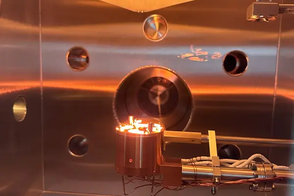
The Nikalyte’s EVAP-4 is a compact, four-pocket mini electron beam evaporator designed for research laboratories and small-scale production environments where precision, substrate compatibility, and material flexibility must be achieved within a single platform.
- Low thermal load by design: The EVAP-4 uses a focused electron beam to directly heat the evaporant within a small crucible or rod. Because the source geometry is intentionally compact 57 mm in-vacuum diameter for the EVAP-4 and 34 mm for the EVAP-4C the effective hot surface area is inherently limited. This design significantly reduces radiant heat transfer to the substrate compared with both conventional resistive thermal evaporators and larger e-beam hearth systems. The result is a consistently lower thermal footprint during deposition, supporting temperature-sensitive processes without compromising film formation. [12, 13]
- Four-pocket co-evaporation: The system supports up to four materials simultaneously, with independent pocket control managed through a four-channel power supply. This allows sequential or stacked deposition of complex metal systems such as titanium adhesion layers, platinum diffusion barriers, and gold contact layers within a single vacuum cycle. By eliminating the need to vent between depositions, the EVAP-4 removes one of the most common sources of inter-layer contamination: atmospheric oxidation at exposed interfaces. [12]
- Flux monitoring for repeatable results: Each pocket is equipped with an independent flux monitoring plate positioned above the source. This measures ion current generated during evaporation in real time, providing a direct, quartz crystal microbalance (QCM)-independent indication of deposition rate. For gold, a strong linear relationship between flux and deposition rate is observed, with R² > 0.98 above 65 W. This level of stability allows flux to be used as a primary control signal, particularly in co-evaporation workflows where independent monitoring of each pocket is critical for repeatability. [12]
- Material range from noble metals to refractory compounds: The EVAP-4 has been validated across a broad material set spanning noble metals, transition metals, and refractory elements. Silver achieves deposition rates of 40 Å/s at 70 W, copper reaches 60 Å/s at 146 W, and chromium maintains stable operation at 1.7 Å/s over extended runs. Materials that are typically inaccessible via resistive thermal evaporation such as platinum and tungsten can be deposited using adapted geometries, including carbon support sleeves and shaped rod configurations. Tungsten, for example, achieves stable deposition at 0.075 Å/s at 160 W using a tapered rod and circular filament, as documented in the Nikalyte technical white paper. [12]
- UHV compatibility and full bakeability: The EVAP-4 is designed for ultra-high vacuum operation, achieving base pressures of <5 × 10⁻⁷ mbar for noble metals and <2 × 10⁻⁷ mbar for reactive metals. The system is fully bakeable to 250°C, enabling thorough outgassing prior to deposition runs involving sensitive materials or surface-critical applications. This level of vacuum integrity supports reproducible thin-film growth in research-grade environments where contamination control is essential.
- Compact form factor with full research capability: Conventional e-beam hearth systems often require significant capital investment, dedicated facility infrastructure, and complex operational workflows. The EVAP-4 retains the same core principle localised electron beam heating of source material but integrates it into a compact platform compatible with a 4.5-inch ConFlat flange. For laboratories working within space, budget, or infrastructure constraints, it provides a practical route to high-quality e-beam evaporation without the overhead of a full-scale deposition system. [12]
Conclusion
A thermal evaporator remains a reliable and widely used tool for straightforward metal deposition on robust substrates. However, its limitations become more apparent in demanding applications involving photoresist-patterned wafers, temperature-sensitive materials, ultra-clean film requirements, or refractory metals. In these cases, the inherent heat load from resistive heating, along with potential contamination pathways, can shift from being a background variable to a direct process constraint. Knowing where these limits sit and selecting equipment designed to operate within them is often what separates repeatable deposition from iterative troubleshooting.
The Nikalyte EVAP-4 Mini E-Beam Evaporator is engineered specifically around these constraints. It delivers low radiant heat load through a compact electron beam source geometry, supports multi-material deposition within a single vacuum cycle, and incorporates real-time flux monitoring for improved process control. With full UHV compatibility, it is designed for environments where film purity, interface control, and thermal sensitivity are not optional considerations but core requirements. For laboratories operating at the edge of conventional thermal evaporation capability, it represents a practical next step in precision thin-film deposition.
Contact Nikalyte to discuss your deposition requirements or download the EVAP-4 white paper for full technical data.
References
- Toma, F. T. Z. Z., Rahman, M. S., Hussain, K. M. A., & Ahmed, S. (2024). Thin film deposition techniques: A comprehensive review. Journal of Modern Nanotechnology, 4(6). https://doi.org/10.53964/jmn.2024006
- Lovett, A. J., Kursumovic, A., & MacManus-Driscoll, J. L. (2024). Lithium loss in vacuum deposited thin films. ACS Energy Letters, 9(4), 1753–1758. https://doi.org/10.1021/acsenergylett.4c00153
- Nikalyte Ltd. (2024). Lift-off process for nanoscale devices using e-beam deposition. https://www.nikalyte.com/lift-off-process-for-nanoscale-devices-using-e-beam-deposition/
- Microchemicals GmbH. (n.d.). Lift-off processes with photoresist [Application note]. https://www.microchemicals.com/dokumente/application_notes/lift_off_photoresist.pdf
- Elshenety, A., Kucuk, M. M., & Yilmaz, M. (2025). High thickness material lift-off using multi-layer photoresist. Journal of Micromechanics and Microengineering, 35(2), 025012. https://doi.org/10.1088/1361-6439/adac6b
- Angstrom Engineering. (2025). Troubleshooting electron beam evaporation processes. https://angstromengineering.com/troubleshooting-electron-beam-evaporation-processes/
- Qerimi, D., Panici, G., Jain, A., Jacobson, D., & Ruzic, D. N. (2021). Role of electron and ion irradiation in a reliable lift-off process with electron beam evaporation and a bilayer PMMA resist system. Journal of Vacuum Science & Technology B, 39(5), 052601. https://doi.org/10.1116/6.0001130
- Sahin, O., Albayrak, O. M., & Yapici, M. K. (2024). Optimization of e-beam lithography parameters for nanofabrication of sub-50 nm gold nanowires and nanogaps based on a bilayer lift-off process. Nanotechnology, 35(39), 395301. https://doi.org/10.1088/1361-6528/ad5e89
- SRI International Foundry. (2026). Film deposition services: E-beam evaporation. https://www.srifoundry.com/services/film-deposition/
- Chen, Y.-L., & Wang, P.-J. (2023). Study of ion-assisted E-beam evaporation coating process on chirped mirrors. Coatings, 13(2), 356. https://doi.org/10.3390/coatings13020356
- Lackner, P., Choi, J. I. J., Diebold, U., & Schmid, M. (2017). Construction and evaluation of an ultrahigh-vacuum-compatible sputter deposition source. arXiv. https://doi.org/10.48550/arXiv.1710.06377
- Joseph, J., Broadley, V., Saranu, S. R., & Vaughan, M. (2025). Advanced thin film deposition with the EVAP-4 mini e-beam evaporator: A comprehensive technical analysis [White paper]. Nikalyte Ltd. https://www.nikalyte.com/wp-content/uploads/Advanced-thin-film-deposition-with-the-EVAP-4-mini-e-beam-evaporator-A-comprehensive-technical-analysis.pdf
- Nikalyte Ltd. (n.d.). Mini e-beam evaporator (EVAP-4). https://www.nikalyte.com/uhv-e-beam-source/